
NEWS
2023-5-13
Notice of Website Renewal
2019-1-25
Notice of inauguration of CEO
We, Echo Giken, will continue to create and provide high quality products,
pursue safety and hygiene and environmentally friendly cleaning technology,
and advance and develop cleaning technology under the motto of "customer trust and satisfaction".
We will continue to research and develop to the world of 1nm/2nm nano-technology and provide it to our customers for their manufacturing process lines.
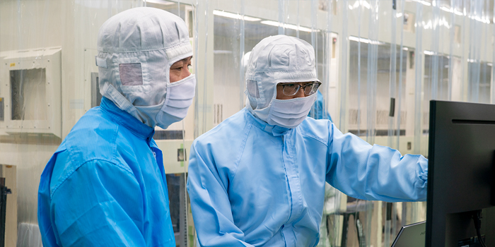
Cleaning equipment that cleans the best wafers at the nano-level. Even nano-level debris is a large piece of debris in the process.
It is never visible to the naked eye. We are challenging the limits of silicon wafers,
which continue to shrink in size, together with our customers. We provide the highest level equipment to wafer manufacturers around the world.
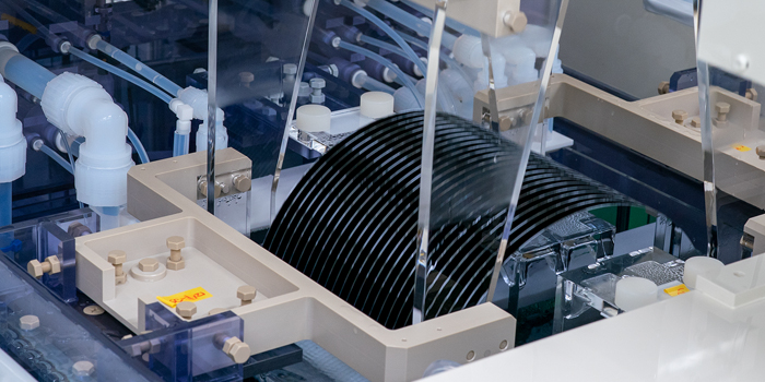
Our final cleaning equipment continues to contribute to the final process in the bare wafer manufacturing process.
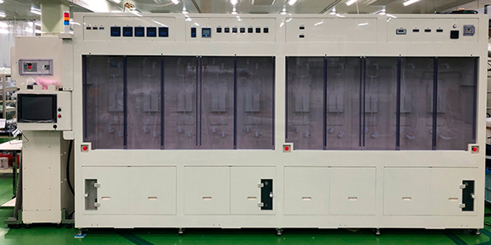
With the recent miniaturization of semiconductors, filters used in various semiconductor manufacturing processes are required to be of higher cleanliness. We propose specialized equipment that can achieve advanced filter cleaning in response to various customer requirements.
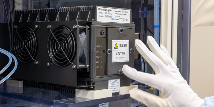
“measure the future with measure.”
Light absorption type In-line design So strong
ChemicAlyzer is a densitometer for liquid components that applies the light absorption principle and realizes continuous measurement with an in-line design.
Since 1990, when KURABO started our business as a pioneer of infrared liquid component densitometers, we have supported quality and chemical concentration control by "responding to measurement needs" in the ever-evolving semiconductor device manufacturing process with our abundant know-how and technologies. We will continue to support cutting-edge processes and special chemical solutions in the future.
We will continue to contribute to the optimization of manufacturing processes by flexibly responding to cutting-edge processes and special chemicals and "responding to measurement needs one step further" through high-precision chemical concentration measurement.